Actualités >
Retour à la liste des actualités
 The network features asymmetrical (nano)electrodes to obtain a highly efficient photoelectric conversion, paving the way for potential uses at the intersection of optoelectronics and nanotechnology. This work appeared in the journal Nature Nanotechnology.
Supramolecular nanowires made from self-assembled semi-conductive organic building blocks are components adapted for developing highly effective optoelectronic devices. This level of performance is possible due to their superior optical (absorption of and sensitivity to light), electronic (transporting charge carriers) and morphological (surface-to-volume ratio) properties. Making devices from organic nanowires remains difficult, however, due mainly to a lack of control over the interface between the nanowire and the electrodes.
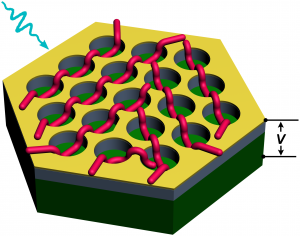
A European team of researchers from Strasbourg and Nova Gorica has thus developed a new strategy to simultaneously connect hundreds of supramolecular nanowires to nanoelectrodes with different energy levels. This connection is necessary to ensure a direct, efficient harvesting of light energy. To this end, a honeycomb structure of millions of well-like nanoeletrodes has been designed and made using a step-by-step approach that combines nanosphere lithography and reactive ion etching. A commercially available n-type organic semi-conductor (electron transporter) was chosen as a prototypical building block, as it is known for forming strong supramolecular nanowires.
After the PTCDI-C8 nanowires were self-assembled, placed on the nanomesh structure and thermally treated in an inert atmosphere, a photovoltaic effect attributed to light absorption by the supramolecular nanowires was observed. It is important to note that the width and thickness of the nanowires, as well as the diameter and the depth of the nanowells, can easily be adjusted.
The researchers then managed to selectively modify the bottom electrode by placing a thin layer of a p-type (hole-transporting) semi-conducting polymer on the silicon surface inside the nanowells, forming a p–n junction with the PTCDI-C8 supramolecular nanowires without altering the morphology of the nanomesh. After optimisation, the photonic devices exhibited outstanding characteristics, such as a high signal-to-noise ratio (107), an ultrafast photoresponse time (10 ns) and an external quantum efficiency exceeding 55%.
These findings are of great importance for creating high-performance optoelectronic devices based on organic nanostructures (e.g. nanowire-based light-emitting diodes or spin valves), by filling the gap between bottom-up nanostructured semiconductors and macroscopic optoelectronic applications.
Lei Zhang, Xiaolan Zhong, Egon Pavlica, Songlin Li, Alexander Klekachev, Gvido Bratina, Thomas W. Ebbesen, Emanuele Orgiu & Paolo Samorì
A nanomesh scaffold for supramolecular nanowire optoelectronic devices
Nature Nanotechnology 25 juillet 2016
DOI : 10.1038/nnano.2016.125
